Abstract
This paper presents an active impedance matching scheme that tries to optimize electrical power transfer and acoustic reflectivity in ultrasound transducers. Leveraging negative capacitance-based impedance matching would potentially improve the bandwidth and electrical power transfer while minimizing acoustic reflection of transducer elements and improve uniformity while reducing acoustic crosstalk of transducer arrays. A 16-element transceiver front-end is designed which employs an element-level active capacitive impedance cancellation scheme using an element-level negative impedance converter. The ASIC fabricated in 180-nm HVBCD technology provides high-voltage pulses up to 60 V consuming 3.6 mW and occupying 2.5 mm2. The front-end ASIC is used with a 1-D capacitive micromachined ultrasonic transducer (CMUT) array and its acoustical reflectivity reduction and imaging capabilities have successfully been demonstrated through pulse-echo measurements and acoustic imaging experiments.
Keywords: Capacitive micromachined ultrasonic transducer (CMUT), acoustic reflectivity, negative capacitance (NC), impedance matching, ASIC, ultrasound transceiver (US-TRX), capacitive cancellation, crosstalk, HV pulser, array uniformity
I. INTRODUCTION
Integration of ultrasonic transducer arrays with their associated electronics has transformed a variety of ultrasound imaging and sensing applications, particularly those that benefit from the integration of 1-D and 2-D imaging arrays with their electronics such as Intravascular Ultrasound [1], Intracardiac Echocardiography [2], [3], transesophageal Echocardiography [4], and Point-of-care Ultrasound [5], [6]. Micromachined arrays are interfaced with their readout electronics for signal detection and amplification [7]–[9]. However, typical voltage- or current-based low-noise amplifiers as the first stage in the readout interface electronics introduce mismatches into terminating transducer array elements and cause electrical and acoustic reflections leading to reverberations, eventually degrading the overall transducer array and imaging performance. Employing proper impedance matching can preserve the signal-to-noise ratio (SNR) and minimize acoustic reflections.
There are a few research works in the literature that focus on this issue and address it comprehensively. For instance, employing backing materials has been reported for improving acoustic reflections and signal detection. However, such a solution is desired for a medium with a known target or for a narrow frequency band, and its tunability is limited [10], [11]. In addition, a few studies report manipulating terminations electronically such as adding a resistive termination [10], [12]. As a straightforward approach to tuning capacitive transducers, inductive tuning has been reported but has its own limitations including narrow bandwidths and large sizes. Post-processing techniques on the echo data in the backend have also been proposed for improving acoustic reflections [13] which cannot be applied to the general context due to their limited performance. Therefore, novel approaches are needed to provide feasible broadband matching and to distinguish the trade-off between electrical power transfer and acoustic reflectivity and the optimum termination for those conditions. A recent article [14] discusses the trade-off between these two aforementioned conditions and a detailed analysis has been reported employing a CMUT model and an experimentally-validated model for CMUT elements.
Negating the capacitive reactance of the ultrasound transducer element provides a broad bandwidth for CMUT element operation regardless of the CMUT operation regime. Adding such a matching circuitry not only minimizes acoustic reflections but also improves signal detection. It can be realized by leveraging active circuitry for negative capacitor implementation and is particularly of high importance because of its integration capability and electronic tunability, providing higher miniaturization and improving overall system performance.
In this article which is an extension of [15], the analysis of adding a negative capacitance-based impedance matching is presented with the focus mostly on the circuit design and performance analysis validated by experimental results. Section II presents the detailed analysis of adding the matching circuitry including signal and noise analyses. Presented in Section III is the proposed architecture including the element-level impedance matching and the details of the front-end design for interfacing a 16-element CMUT array. The electrical and acoustic characterization along with the imaging experiment are discussed in Section IV, and the concluding remarks are presented in Section V.
II. Impedance Matching Analysis
A. Electrical Power Transfer vs Acoustic Reflectivity
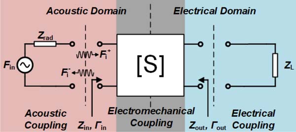
In order to evaluate the power transfer and acoustic reflectivity in the receive mode, CMUT elements can be modeled as linear time-invariant networks and can be interpreted by their scattering parameters [16]. As shown in Fig. 1, an ultrasound transducer element is an electro-acoustic converter whose reflection coefficients are defined in two different domains, i.e., acoustic and electrical. Similar to any transducer, reflection coefficients describe the effectiveness of coupling. In Fig. 1, the acoustic reflection coefficient in the acoustic domain is defined at the interface of a transducer and the radiation medium and is given by
| (1) |
where Zin is the input mechanical impedance of the transducer at the mechanical port and Zrad is the radiation impedance of the medium [17], [18]. On the contrary, the power reflection coefficient in the electrical domain is defined at the interface of a transducer and the readout circuitry and is given by
| (2) |
where * denotes complex conjugate, Zout is the output electrical impedance of the transducer at the electrical port, and ZL is the load impedance representing the input impedance of the readout circuitry. According to reflection equations, the electrical power reflection is minimized when the complex conjugate condition in the electrical domain is satisfied while the acoustic reflection is minimized when the input mechanical impedance of the transducer matches the radiation impedance of the medium. The termination provided by the readout circuitry affects both reflection coefficients since an ultrasonic transducer connects the electrical domain to the acoustic domain through electromechanical coupling and subtly one may notice that the optimum termination for minimizing electrical power reflections does not coincide with the optimum load for optimum acoustic reflection.
Fig. 1.
A two-port network model for a transducer element.
Adding a matching circuitry at the electrical port can manipulate reflection coefficients for achieving optimum conditions of electrical and acoustic matching [19]. To delve into this, exploring (1) and (2) requires to use of an equivalent circuit model for ultrasonic transducers. Without loss of generality, Fig. 2 shows the equivalent circuit model for a 1-D CMUT element. Zrad and Zmem are the total impedances which are the normalized impedances multiplied by the effective area.1 In this small-signal equivalent circuit model, the electromechanical transformation is represented by its ratio, n = VdcC0/g, where C0 is the CMUT capacitance, g is the gap between CMUT plates, and Vdc is the applied DC bias. The spring softening due to the electromechanical coupling with the applied bias is represented by the −C0 element.
Fig. 2.
Mason’s small-signal equivalent circuit for a CMUT element in the receive mode. Zrad and Zmem are the total impedances which are the normalized impedances multiplied by the effective area.
The role of a matching circuitry at the electrical interface is mainly negating the effect of the capacitive reactance of the CMUT element. Knowing the inefficiency of inductive matching, a negative capacitor can provide a better matching. Given a negative capacitor and an ohmic load connected to the CMUT element, the electrical power reflection coefficient is given by
| (3) |
where is a complex conjugate of the output electrical impedance of the CMUT element including the negative capacitor, −C. The maximum electrical power transmission requires minimizing the electrical power reflection. The optimum ohmic load can, therefore, be expressed as
| (4) |
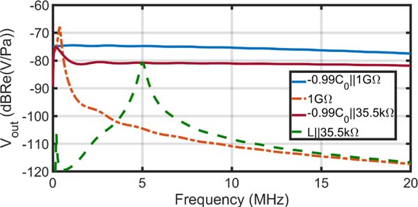
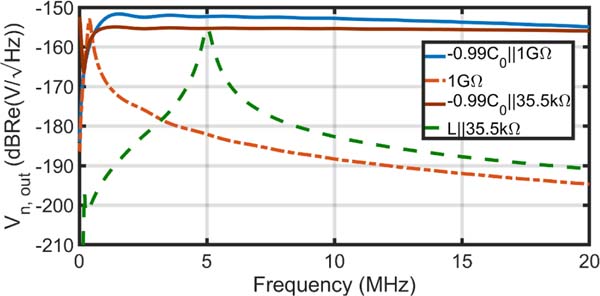
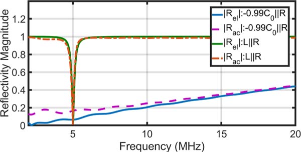
where is the complex conjugate of the short-circuit mechanical impedance. For minimizing the acoustic reflection, however, a closed-form expression is not trivial. It is noteworthy to mention that these two optimum ohmic load values are not equal and this introduces a trade-off in the design. Optimum load values for minimizing acoustic and electrical reflections depend on the CMUT design. To illustrate these concepts and variations, the equivalent circuit model in Fig. 2 is used to evaluate a 5-MHz 64-membrane CMUT element. The performed analysis using C0 = 21.65 pF and L = 46.79 μH shows that adding a negative capacitor can provide a preferred response over a broad bandwidth, improving the acoustic reflectivity while the degradation in SNR can be acceptable (~3 dB) even in the worst-case scenario. As shown in Fig. 3, the inductive matching has provided a narrowband response around the center frequency and the short circuit termination attenuates the output signal over the desired bandwidth. Adding a negative capacitor with an ohmic termination can provide similar broadband responses with respect to only negative capacitors but it significantly reduces acoustic reflectivity. In contrast, −C matching provides signal gain and bandwidth with no SNR loss while having higher acoustic and electrical reflectivity. The noise response shows similar trends in Fig. 4. The negative capacitor with an ohmic termination has a constant noise response over the frequency which is similar to the only negative capacitor response and has an improvement of ~5 dB in noise reduction. It is noteworthy to mention that the actual SNR depends on the active circuitry and transmit/receive switches in the receive path. As expected and shown in Fig. 5, adding a negative capacitor with an ohmic termination improves both electrical and acoustic reflectivity over a broad bandwidth and the ohmic termination can be tuned to maximize the desired reflectivity. Overall, an expected improvement of ~14 dB can be achieved for the lower band up to 10 MHz while it decreases to 8 dB for up to 20 MHz.
Fig. 3.
The output voltage for different terminations. A 5-MHz 64-membrane CMUT element is used for analysis. −C matching can provide a broadband response.
Fig. 4.
The output noise for different terminations. A 5-MHz 64-membrane CMUT element is used for analysis. −C matching can provide a flat noise response with noise improvement.
Fig. 5.
Electrical (Rel) and acoustic (Rac) reflectivity for different terminations. A 5-MHz 64-membrane CMUT element is used for analysis. −C matching improves both acoustic and electrical reflectivity over a broad bandwidth.
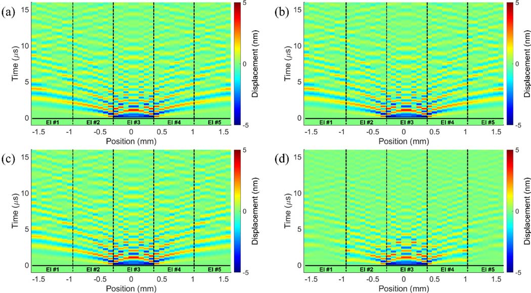
Another impact of impedance matching is on the acoustic crosstalk in the array [20]–[22]. Acoustic crosstalk, basically non-ideal coupling between array elements, degrades the bandwidth of the individual elements as well as the array imaging performance. For crosstalk analysis, a 5-element CMUT array is used whose elements have properties similar to the one used for the single-element analysis, and the calculations are performed using a custom-developed simulation program described in [23]. The center element is pulsed, and the crosstalk is analyzed through the displacement of the neighboring CMUT membranes. The center element is terminated at the short circuit while the remaining elements are terminated with short circuit (~0.1 Ω), open circuit (~1 GΩ), inductive matching (50 μH||70 kΩ), and negative capacitance matching (−20.57 pF||600 kΩ). Illustrated in Figs. 6(a)–6(d) are the crosstalk analysis results for different terminations. As clearly seen in the figures, the spurious displacement is significantly reduced both in space (lateral axis) and in time (vertical axis) for Fig. 6(d). Considering the average displacement of each element, the simulated displacement of the farthest element with respect to the center achieves the greatest improvement when a negative capacitance matching is used. This is expected as the edge element of the array has a rigid surface beyond it and hence it gets impacted more by the immediate reflections at that boundary condition. For instance, when one considers the time-averaged displacement over the whole time period, the crosstalk is reduced by more than 10× for negative capacitance matching with respect to no matching. This reduction in crosstalk is improved by more than 12.5× with respect to short circuit or inductive matching. Therefore, with negative capacitive matching, one expects improvements in crosstalk and image quality.
Fig. 6.
Crosstalk analysis results for different terminations: (a) short circuit (~0.1 Ω), (b) inductive matching (50 μH||70 kΩ), (c) open circuit (~1 GΩ), (d) negative capacitance matching (−20.57 pF||600 kΩ). Considering the average displacement of each element, the displacement of the farthest element with respect to the center achieves the greatest improvement when a negative capacitance matching is used.
B. Circuit Analysis
Adding an ideal negative capacitor to a CMUT receiver circuit would potentially increase the SNR or its degradation can be negligible. However, there are other factors that have an impact on the SNR and a detailed analysis is required. In Section II.A, a noiseless negative capacitor is assumed for exploring the impact of negating the capacitive reactance of the CMUT element. The realization of a negative capacitor requires active circuitries that introduce new noise sources in the calculation [24], [25]. Moreover, a receiver path includes a high-voltage switch in series with the CMUT element that turns off the receive path during transmit mode where the CMUT element is used as both receive and transmit element. In order to analyze the noise performance, two different cases are studied. In one case the low noise amplifier structure is different and the second one covers a more favorable case. For the noise analysis, the CMUT model consists of a noise source, the mechanical impedance transferred to the electrical domain, and the CMUT capacitance. In the first case, a trans-impedance amplifier is considered that can provide ohmic terminations with small values. The trans-impedance amplifier uses a common model in which a resistive-feedback structure is applied [26]. The structure model includes a noiseless amplifier with its current and voltage noise sources. In addition, the negative capacitor model consists of a noiseless negative capacitor with current and voltage noise sources. Adding both current and voltage noise sources guarantees any correlation, but one may want to remove one of the noise sources, depending on the topology. In other words, it can be proved that both voltage and current sources are essentially sufficient for representing the noise of linear CMOS circuits [27]. This is necessary since adding only a voltage noise source for circuitry with a finite input impedance implies an incorrect result that the output noise vanishes when the source impedance becomes large. Adding a parallel current noise source, therefore, resolves this issue since the current noise source still produces noise at the input in the case that the source impedance of the preceding stage is surmised to have a large value.
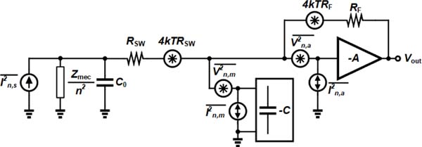
Fig. 7 shows the equivalent circuit for noise calculation in which the noise is derived for the input node. For simplicity, Zmech/n2 and the input impedance of TIA are replaced by R0 and RL in the following calculations. The total current noise power spectral density (PSD) at the interface of the CMUT and electronics is given by
| (5) |
where the noise source of the switch is neglected. To include effect of a switch noise source, a switch resistor in series with a voltage noise source is added to the interface [see Fig. 7]. The contribution of the switch noise to the overall input-referred noise is given by
| (6) |
Fig. 7.
The equivalent circuit for the noise analysis. A switch resistor and its associated voltage noise source are added to the equivalent circuit model.
To have a better insight into the signal-to-noise ratio (SNR), signal analysis is performed. Following the same assumption as stated for the noise analysis, the signal ratio is given by
| (7) |
where S2 and S1 are the signal power for the case with the negative capacitor and the case without the negative capacitor, respectively. Adding the switch resistor to the calculations, the signal ratio is given by
| (8) |
In the general case, larger resistors are required for matching trade-offs. Therefore, a voltage amplifier is used for signal amplification with high input impedance, and a resistor is added at the interface for matching. Assuming the same voltage and current noise sources for the voltage amplifier as the amplifier A’s noise sources in Fig. 7, the input current noise at the interface is similar to (5), where the resistor RL is replaced with the matching resistor. Consequently, (6)–(8) are valid for the general case. It is worth noting that the main contributors are the transducer element, the switch, and the termination resistor among all noise sources. Certainly, the C2ω2 term associated with the voltage noise of the amplifier increases its contribution to the total input current noise at higher frequencies. If the transducer element noise contribution dominates which most likely happens in the case of large 1-D CMUT elements, the SNR increases with respect to an open-circuit or a short-circuit termination.
III. Circuit Architecture
A. Overview
A typical ultrasound array imaging system front-end uses high voltage pulsers for pressure signal generation and high voltage switches to protect the receiver amplifiers connected to each array element. In this particular application of intracranial ultrasound considered here, the imaging speed is not that critical as low frame rate imaging of the stationary brain tissue is targeted. Therefore, a single receiver chain is used after a low voltage multiplexer as shown in the transceiver front-end block diagram of Fig. 8. This structure is suitable to study negative capacitance matching as this feature can be turned on and off to study its impact on overall system performance.
Fig. 8.
Simplified block diagram of the proposed architecture of the transceiver front-end with element-level impedance matching for low frame rate applications such as intracranial ultrasound.
B. Front-End Design
The proposed transceiver front-end includes a negative capacitor at the receiver which compensates the total capacitance at the interface node including the CMUT capacitance and any parasitic presented at the interface node. A transmitter path consists of level-shifters and a high-voltage pulser is used for exciting each element. A receiver path consists of an element-level negative impedance converter, a low-noise trans-impedance amplifier with programmable time-gain compensation, and a buffer for driving the output node before connecting to a digitizer.
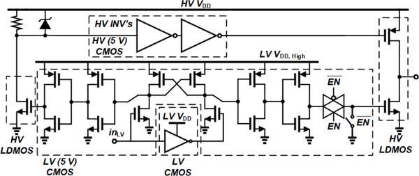
To generate sufficient pressure waves emitted from the CMUT element, high-voltage excitation is required. On-chip high voltage pulses are available thanks to the high-voltage technology nodes. However, added extra layers for high-voltage operation make high-voltage transistors bulkier than their standard CMOS transistors thus occupying a larger silicon area. Fig. 9 shows the schematic of the high-voltage pulser. The generated low-voltage pulse widths with an amplitude of 1.8 V from the control line (in general from a beamformer) go through a low-voltage inverter and then a cross-coupled regenerative pair provides high and low voltages for level shifters in which the pulses are shifted up to provide pulses that have an amplitude of 5 V, the operating gate-source voltage for high-voltage transistors. These 5-V pulses are sufficient for driving the pull-up and pull-down transistors at the output stage. The laterally-diffused MOS transistors at the output stage tolerate much larger drain-source breakdown voltages. Employing a high-voltage design, this pulser generates unipolar pulses up to 60 V, driving CMUT elements up to 5 MHz for this particular design.
Fig. 9.
The schematic of the proposed high-voltage pulser. The output stage uses LDMOS transistors to tolerate high-voltage pulses. Low-voltage and high-voltage transistors are marked in the schematic.
Each transducer element includes a high-voltage switch circuitry to isolate the receiver path from high-voltage pulses. A high-voltage transistor is in series with the transducer element and the low-noise amplifier. The on-resistance introduced by the high-voltage switch compromises the presented impedance at the CMUT element output and the frequency response and overall noise of the receiver chain. Smaller on-resistances decrease the switch effect while requiring larger device sizes. On the other hand, larger devices add larger parasitics degrading the noise performance and frequency response.
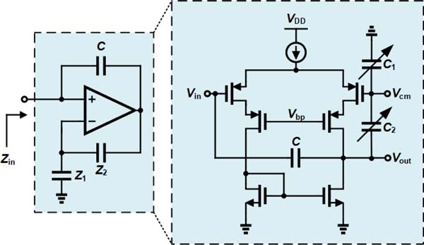
To realize a negative capacitor, one may want to use an impedance converter employing positive feedback. A positive-feedback OpAmp is employed as illustrated in Fig. 10. Z1 and Z2 can form a resistive or capacitive divider.1 To calculate the input impedance, Zin, offered by this circuit, one surmises that the OpAmp has a gain of A and one pole (first-order frequency response, Hence, the input impedance is given by
| (9) |
In a realistic case, the OpAmp gain is large enough (A >> 1) and the simplified input impedance is given by
| (10) |
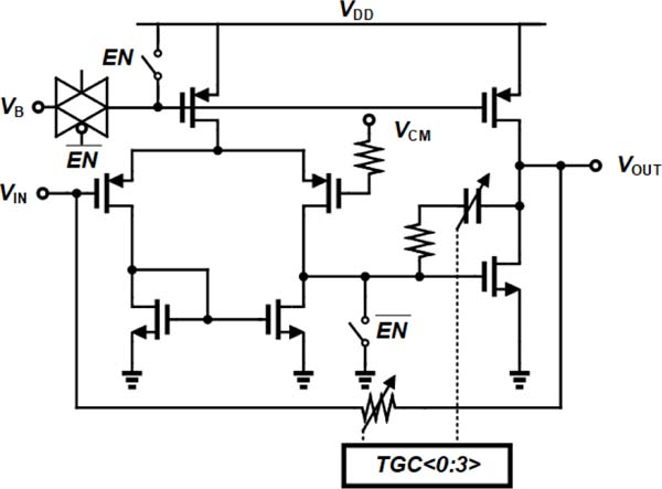
For achieving −25 pF of capacitance, a unit capacitor of 800 fF is used. As this structure introduces a positive pole in the frequency response of the negative capacitor circuitry, additional precautions are required to maintain the proper operation of the negative capacitor and avoid stability issues. A trans-impedance amplifier is employed in the receiver chain to convert the current signal received from the transducer element to a voltage signal. The receiver chain is ended by a buffer for driving the output node before digitization. The trans-impedance schematic is depicted in Fig. 11 where a two-stage amplification is used in which a miller capacitance compensates for the frequency response. It leverages time-gain compensation by adding additional circuitry controlled by two bits.
Fig. 10.
The schematic of the proposed negative capacitor. A capacitive ratio is used for tuning the negative capacitor.
Fig. 11.
The schematic of the trans-impedance amplifier with miller . compensation. A 2-bit control is used for time-gain compensation.
IV. Experimental Results and Discussion
The proof-of-concept front-end SoC prototype for intracranial ultrasound imaging, including the element-level impedance matching technique, has been fabricated in 180-nm HV BCD technology. Recalling low frame-rate imaging, the SoC consists of 16 transmitters and HV isolation while sharing one receiver path and interfaces with a 16-element 1-D CMUT array supplied from three voltage lines. As illustrated in Fig. 12, the ASIC occupies 3.16 mm × 0.822 mm including the bonding pads with an average power consumption of 3.6 mW. The floor plan of each transmitter and HV isolation designed for 160-μm-pitch of a 1-D CMUT array occupies 0.08 mm2 of the silicon area.
Fig. 12.
Die microphotograph fabricated in 180-nm HV BCD technology (left); Edge of 1-D CMUT array (right).
A. Electrical Characterization
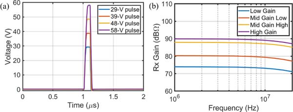
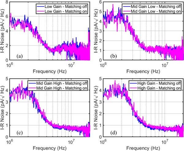
For electrical characterization, the ASIC was wire bonded to a daughter printed circuit board (PCB). Each transmitter was tested separately, and control signals with pulse widths of 100 ns were applied to the pulsers while the receiver chain was deactivated. The measured unipolar pulses are shown in Fig. 13(a) with different amplitudes of up to 58 V and a pulse width of 100 ns. For the receiver chain measurements, the transmitters were deactivated and the CMUT array was used in the collapsed mode.1 The capacitance was in the 50–55 pF range for the DC bias in the 100–140 V range. The frequency response of the receiver chain was measured by adding the proper input signal directly. The gain of the receiver chain is shown in Fig. 13(b) for four different gain settings controlled by two bits. Note that the CMUT element was not connected to the receiver chain for gain measurements. Fig. 14 illustrates the noise performance of the receiver chain for different gain settings. The CMUT element was then connected to the receiver chain for noise measurements with and without negative capacitance matching and at different gain levels. As depicted in Fig. 14, noise measurements showed no discernible degradation in noise performance with matching for any of the gain settings, indicating that the noise is degraded by the large CMUT capacitance. That is, the noise performance of the receiver path hinges essentially upon the CMUT element in this case.
Fig. 13.
(a) The measured pulses of up to 58 V generated by the pulser with a pulse width of 100 ns, (b) The measured frequency response of the RX chain with the variable-gain TIA (excluding the CMUT element).
Fig. 14.
The measured input-referred noise of the RX chain with the variable-gain TIA (including the CMUT element).
B. Acoustic Characterization
For acoustic characterization of the designed ASIC along with the CMUT array, a commercially available 16-element CMUT array (PHILIPS model CM-12) was wire bonded to the chip. Pulse-echo responses of all elements were collected. As shown in Fig. 15, the first element was excited and the responses of all elements were collected in the first experiment. A hard flat reflector was used for high echo signals. It shows that the frequency responses of the elements were improved in terms of both bandwidth and uniformity. As shown, a tighter distribution was observed and ~3–4 dB increase in the frequency response at higher frequencies pushed the upper cut-off frequency further resulting in bandwidth improvement achieved in the 1.5–5 MHz range.
Fig. 15.
The measured frequency response of the array elements collected from pulse-echo measurements. The first element was excited, and the responses of all elements were collected with and without matching. A hard flat reflector was used for high echo signals.
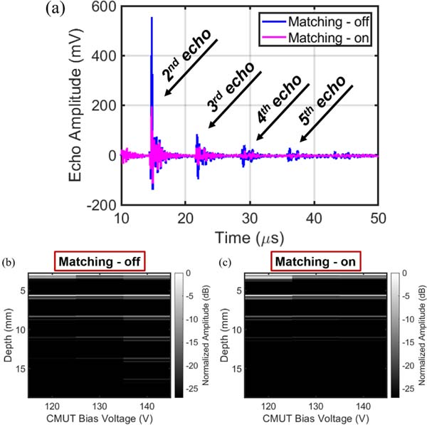
A critical experiment to evaluate the impact of negative capacitance matching is the pulse-echo measurement using one of the array elements. A CMUT element with 120-V DC bias was used in front of a close target. As illustrated in Fig. 16, the echo signal received from the CMUT element terminated with negative capacitance-based matching reduces the reverberations and the second detected echo decreases to ~200 mV from ≥550 mV in the case that there is no matching applied. Reduction in multiple echo levels (reverberations) significantly reduces the acoustic noise floor resulting in increased sensitivity of the transducer element. To explore the acoustic reflectivity with respect to the CMUT DC bias, echo amplitudes of all elements were collected with and without matching for different DC bias values. The echo envelopes are shown in Figs. 16(b) and 16(c) where 0 dB describes the maximum for each bias level normalized to its maximum. Compared to broadband matching, the readout without matching exhibits longer echoes, thus elongating the unwanted response. A significant reduction in acoustic reflectivity was observed where adding element level impedance matching reduces the echo signals drastically. Particularly at 140-V DC bias, the echo signals after the third echo are negligible. It is noteworthy to mention that proper matching resulted in uniformity of the system for all array elements at each bias level. Furthermore, this significant improvement has been obtained with sub-optimal negative capacitance matching, as the negative capacitance circuit provides ~25 pF of compensation while the CMUT capacitance is in the 50–55 pF range.
Fig. 16.
(a) Measured echoes in the pulse-echo experiment (FC70/air interface with the 2.7-mm height of FC70), (b) the effect of the proposed matching on multiple echoes (2nd echo and the next ones) vs. CMUT bias utilizing single-element US TRX. CMUT array operates in the collapsed mode for each of the 120-V, 130-V, and 140-V levels.
C. Imaging Experiment
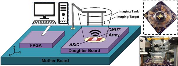
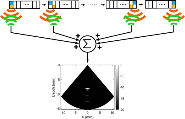
As an ultimate experiment to illustrate the impact of broadband matching, the imaging setup illustrated in Fig. 17 was used, where the 16-element CMUT array was employed for imaging a 3-wire custom-made phantom in an FC70 filled imaging tank. FC70 is a dielectric liquid with an acoustic impedance similar to water and acoustic attenuation of ~0.1–0.8 dB/mm/MHz at ~2–5 MHz. This dielectric fluid provides electrical isolation for uncoated CMUT dies. The phantom was made of wires with a thickness of 600 μm and spacing of 2.3 mm, and the closest one was placed 8 mm away from the CMUT array, as shown in Fig. 17. For performing the imaging experiment, the synthetic aperture method was employed where each transducer element was used as a transmitter and received echo signals were collected from all transducer elements, as depicted in Fig. 18. For image reconstruction [28], offline dynamic transmit and receive beamforming was applied and the intensity of each image pixel was calculated. Leveraging the standard delay-and-sum beamforming, the calculated pixel intensity in the Cartesian coordinates is given by
| (11) |
where (x,y) is the pixel coordinates and S is the sampled echo data. K is the sample index, and di and dj are the distance between the object and the active transmitter element and the object and the active receiver element, respectively.
Fig. 17.
The test setup for the imaging experiment. A 3-wire custom-made phantom is used as the imaging target.
Fig. 18.
Synthetic aperture (SA) imaging method.
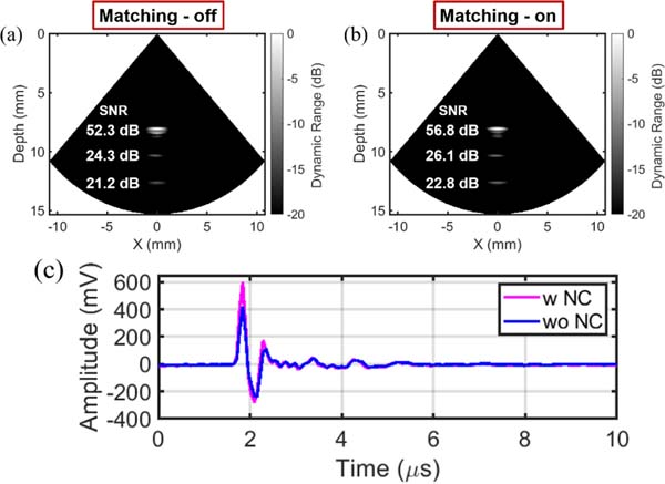
Imaging experiments were performed for two cases. In the first case, the US transceiver was used while the matching was off. In the second case, the US transceiver collected pulse-echo data while the negative capacitance-based matching was employed. Applying a CMUT bias of 110 V, the reconstructed images are shown in Fig. 19 with a 20-dB dynamic range. As expected, adding matching improved resolution and image contrast. Also, adding a negative capacitor improves the power transfer, in this case, resulting in an improved SNR. The first echo amplitude for both cases is plotted and depicted in Fig. 19(c) where the peak amplitude increased by more than 200 mV (in this case 50%) when the US transceiver turned element-level impedance matching on. The image SNR analysis shows that the SNR was improved by 4.5 dB, 1.8 dB, and 1.6 dB for the first, second, and third wire, respectively. In addition to the SNR improvement, the axial resolution, which is mainly determined by the bandwidth was improved, as clearly seen for the first target.
Fig. 19.
(a), (b) Imaging results from the 3-wire target (Dynamic Range of 20 dB). The target phantom with the closest depth of 8 mm, wire spacing of 2.3 mm, and the wire thickness of 0.6 mm was immersed in FC70 (acoustic attenuation ~0.1–0.8 dB/mm/MHz at ~2–5 MHz). (c) improving the first received echo from a target at 6 mm with negative capacitance matching.
Table I summarises the performance of this work and compares it with the state-of-the-art ultrasound solutions for various applications. As expected, the performance of the ultrasound imaging systems can be improved by adding a proper impedance matching network for each element.
TABLE I.
Performance Summary and Comparison with the State-of-the-Art
| Specifications | This Worka | [7] | [29] | [30] | [31] |
|---|---|---|---|---|---|
| Technology | 180 nm HV BCD | 350 nm HV CMOS | 180 nm HV BCD | 180 nm HV CMOSb | 180 nm HV CMOS |
| Transducer | CMUT | CMUT | CMUT | CMUT | PZT |
| Element Level Imp. Matching | YES | NO | NO | NO | NO |
| TX/RX Array | 16-TX/1-RX | 56-TX/48-RX | 64 TRX | 4-TX/4-RX | 7 TRX |
| Bandwidth (MHz) | 2–4 | 40 | 7 | 5.2 | 5 |
| Element Cap. Load | 25 pF | 90 fF | 15 pF | 40 pF | 79.9 pF |
| Avg. Power (mW) | 3.6 @ 1.8 V | 20 | 4.9c | 14.3 | N/A |
| Area (mm) | 2.6 | 1.54 | 29.7 | 1.5d | 2 |
| TX Max Pulse (V) | 60 | 30 | NA | 30 | 32 |
| RX Gain (dB) | 74–90 | 106 | 106 | 96.6 | N/A |
| Input-Referred Noise (pA/√Hz) | 2–3 @3 MHz | 0.31@20 MHze | 2 @5 MHz | 1.35 @3 MHzf | N/A |
| Application | Intracranial Ultrasound | Intracardiac Echocardiography | Intracardiac Echocardiography | Medical Ultrasound | Fitness Tracking |
Includes BGR and bias generation circuitry.
Gate-oxide can handle 30-V swing.
It indicates the TIA power consumption.
Excluding the pads
TIA I-R noise with 90-fF CMUT
Calculated based on reported values
V. Conclusion
In this paper, the trade-off between electrical power transfer and acoustic reflectivity has been discussed and the effect of a negative capacitor-based impedance matching has been presented. Design details of the matching network and its noise analysis have been described. Adding an element-level broadband matching network for capacitive transducers improves the transducer performance and it can be compatible with the size constraints in the monolithic integration of electronics with ultrasonic arrays. It reduces acoustic reflectivity and improves the minimum detectable signal that results in SNR improvement and consequently resolution and contrast of ultrasound images. An ASIC designed for intracranial ultrasound imaging verifies the effect of element-level matching through pulse-echo measurements and acoustic imaging experiments.
Acknowledgment
Any opinions, findings, conclusions, or recommendations expressed in this material are those of the authors and do not necessarily reflect the views of the National Institutes of Health.
Footnotes
Note that a capacitive divider is preferred because of silicon implementation.It not only occupies a smaller footprint but also is more robust against the process, voltage, and temperature (PVT) variations.
Note that the CMUT capacitance changes with the DC bias voltage.
Contributor Information
Ahmad Rezvanitabar, School of Electrical and Computer Engineering, Georgia Institute of Technology, Atlanta, GA 30332, USA..
M. Sait Kilinc, School of Electrical and Computer Engineering, Georgia Institute of Technology, Atlanta, GA 30332, USA..
Coskun Tekes, Department of Electrical and Computer Engineering, Kennesaw State University, Marietta, GA 30033, USA..
Evren F. Arkan, G. W. W. School of Mechanical Engineering, Georgia Institute of Technology, Atlanta, GA 30332, USA..
Maysam Ghovanloo, Bionic Sciences Inc., Atlanta, GA, USA..
F. Levent Degertekin, School of Electrical and Computer Engineering and the G. W. W. School of Mechanical Engineering, Georgia Institute of Technology, Atlanta, GA 30332, USA..
References
- [1].Lim J. et al. , “Highly integrated guidewire ultrasound imaging system-on-a-chip,” IEEE J. Solid-State Circuits, vol. 55, no. 5, pp. 1310–1323, May 2020. [DOI] [PMC free article] [PubMed] [Google Scholar]
- [2].Jung G. et al. , “Single-chip reduced-wire CMUT-on-CMOS system for intracardiac echocardiography,” in Proc. IEEE Int. Ultrason. Symp, Oct. 2018, pp. 1–4. [Google Scholar]
- [3].Wildes D. et al. , “4-D ICE: A 2-D array transducer with integrated ASIC in a 10-Fr catheter for real-time 3-D intracardiac echocardiography,” IEEE Trans. Ultrason., Ferroelectr., Freq. Control, vol. 63, no. 12, pp.2159–2173, Dec. 2016. [DOI] [PubMed] [Google Scholar]
- [4].Chen C. et al. , “A front-end ASIC with receive sub-array beamforming integrated with a 32×32 PZT matrix transducer for 3-D transesophageal echocardiography,” IEEE J. Solid-State Circuits, vol. 52, no. 4, pp. 994–1006, Apr. 2017. [Google Scholar]
- [5].Sanchez N. et al. , “34.1 an 8960-element ultrasound-on-chip for point-of-care ultrasound,” in IEEE Int. Solid-State Cir. Conf. Dig. Tech. Papers, Feb. 2021, pp. 480–482. [Google Scholar]
- [6].Bhuyan A, Choe JW, Lee BC, Wygant IO, Nikoozadeh A, Oralkan O, and Khuri-Yakub BT, “Integrated circuits for volumetric ultrasound imaging with 2-d CMUT arrays,” IEEE Transactions on Biomedical Circuits and Systems, vol. 7, no. 6, pp. 796–804, Dec. 2013. [DOI] [PubMed] [Google Scholar]
- [7].Gurun G. et al. , “Single-chip CMUT-on-CMOS front-end system for real-time volumetric IVUS and ICE imaging,” IEEE Trans. Ultrason., Ferroelectr., Freq. Control, vol. 61, no. 2, pp. 239–250, Feb. 2014. [DOI] [PMC free article] [PubMed] [Google Scholar]
- [8].Jiang X, Tang H-Y, Lu Y, Ng EJ, Tsai JM, Boser BE, and Horsley DA, “Ultrasonic fingerprint sensor with transmit beamforming based on a PMUT array bonded to CMOS circuitry,” IEEE Transactions on Ultrasonics, Ferroelectrics, and Frequency Control, vol. 64, no. 9, pp. 1401–1408, Sep. 2017. [DOI] [PubMed] [Google Scholar]
- [9].Zahorian J, Hochman M, Xu T, Satir S, Gurun G, Karaman M, and Degertekin FL, “Monolithic CMUT-on-CMOS integration for intravascular ultrasound applications,” IEEE Transactions on Ultrasonics, Ferroelectrics, and Frequency Control, vol. 58, no. 12, pp. 2659–2667, Dec. 2011. [DOI] [PMC free article] [PubMed] [Google Scholar]
- [10].Mura ML, Lamberti NA, Mauti BL, Caliano G, and Savoia AS, “Acoustic reflectivity minimization in capacitive micromachined ultrasonic transducers (CMUTs),” Ultrasonics, vol. 73, pp. 130–139, Jan. 2017. [DOI] [PubMed] [Google Scholar]
- [11].Huang Y, Haegstrom E, Bayram B, Zhuang X, Ergun AS, hsiang Cheng C, and Khuri-yakub BT, “Comparison of conventional and collapsed region operation of capacitive micromachined ultrasonic transducers,” IEEE Transactions on Ultrasonics, Ferroelectrics, and Frequency Control, vol. 53, no. 10, pp. 1918–1933, Oct. 2006. [DOI] [PubMed] [Google Scholar]
- [12].Nickel M. and Angelsen B, “A new model describing ultrasound reflectivity at the transducer surface,” in Proc. IEEE Ultrasonics Symposium, Nov. 1996, pp. 889–892. [Google Scholar]
- [13].Chang Y-F, Ma Y, Lin C-M, and Lee J-H, “Reverberation reduction in ultrasonic images via predictive deconvolution,” NDT & E International, vol. 41, no. 4, pp. 235–241, June 2008. [Google Scholar]
- [14].Rezvanitabar A, Arkan EF, and Degertekin FL, “Analysis of negative capacitance-based broadband impedance matching for cmuts,” IEEE Transactions on Ultrasonics, Ferroelectrics, and Frequency Control, vol. 68, no. 9, pp. 3042–3052, Sept. 2021. [DOI] [PMC free article] [PubMed] [Google Scholar]
- [15].Rezvanitabar A. et al. , “An ultrasound imaging front-end system-on-a-chip with element-level impedance matching for acoustic reflectivity reduction,” in Proc. IEEE Biomedical Circuits and Systems Conference, Oct. 2021, pp. 01–04. [Google Scholar]
- [16].Kinsler LE, Fundamentals of Acoustics, 4th ed. New York, NY, USA: Wiley, 2000. [Google Scholar]
- [17].Ozgurluk A, Atalar A, Koymen H, and Olcum S, “Radiation impedance of an array of circular capacitive micromachined ultrasonic transducers in collapsed state,” in Proc. IEEE Int. Ultrason. Symp, Oct. 2011, pp. 1020–1023. [Google Scholar]
- [18].Meynier C, Teston F, and Certon D, “A multiscale model for array of capacitive micromachined ultrasonic transducers,” J. Acoust. Soc. Am, vol. 128, no. 5, pp. 2549–2561, Nov. 2010. [DOI] [PubMed] [Google Scholar]
- [19].Kurokawa K, “Power waves and the scattering matrix,” IEEE Trans. Microw. Theory Tech, vol. 13, no. 2, pp. 194–202, Mar. 1965. [Google Scholar]
- [20].Eccardt P-C, Lohfink A, and Garssen H-G, “Analysis of crosstalk between fluid coupled cmut membranes,” in Proc. IEEE Int. Ultrason. Symp, Sep. 2005, pp. 593–596. [Google Scholar]
- [21].Bayram B, Kupnik M, Yaralioglu G, Oralkan O, Ergun A, song Lin D, Wong S, and Khuri-yakub B, “Finite element modeling and experimental characterization of crosstalk in 1-d CMUT arrays,” IEEE Transactions on Ultrasonics, Ferroelectrics and Frequency Control, vol. 54, no. 2, pp. 418–430, Feb. 2007. [DOI] [PubMed] [Google Scholar]
- [22].Zhao Y, Li Z, Li J, Zhao L, Liu Z, Lu D, Li Z, Yuan J, Yang P, Jiang Z, and Carrara S, “Coupling effects of crosstalk and parasitic loss on capacitive micromachined ultrasonic transducers,” IEEE Sensors Journal, vol. 22, no. 4, pp. 3281–3297, Feb. 2022. [Google Scholar]
- [23].Satir S. and Degertekin FL, “A nonlinear lumped model for ultrasound systems using CMUT arrays,” IEEE Transactions on Ultrasonics, Ferroelectrics and Frequency Control, vol. 62, no. 10, pp. 1865–1879, Oct. 2015. [DOI] [PMC free article] [PubMed] [Google Scholar]
- [24].Merrill JL, “Theory of the negative impedance converter,” Bell Syst. Tech. J, vol. 30, no. 1, pp. 88–109, Jan. 1951. [Google Scholar]
- [25].Brennan RL, Viswanathan TR, and Hanson JV, “The CMOS negative impedance converter,” IEEE J. Solid-State Circuits, vol. 23, no. 5, pp. 1272–1275, Oct. 1988. [Google Scholar]
- [26].Razavi B, Design of Analog CMOS Integrated Circuits, 2nd ed. New York, NY, USA: McGraw-Hill Education, 2017. [Google Scholar]
- [27].Abidi AA, “High-frequency noise measurements on FET’s with small dimensions,” IEEE Transactions on Electron Devices, vol. 33, no. 11, pp. 1801–1805, Nov. 1986. [Google Scholar]
- [28].Karaman M. and O’Donnell M, “Subaperture processing for ultrasonic imaging,” IEEE Transactions on Ultrasonics, Ferroelectrics and Frequency Control, vol. 45, no. 1, pp. 126–135, Jan. 1998. [DOI] [PubMed] [Google Scholar]
- [29].Kang E. et al. , “A 2 pA/√Hz transimpedance amplifier for miniature ultrasound probes with 36 dB continuous-time gain compensation,” in IEEE Int. Solid-State Cir. Conf. Dig. Tech. Papers, Feb. 2020, pp. 354–356. [Google Scholar]
- [30].Chen K, Lee H, Chandrakasan AP, and Sodini CG, “Ultrasonic imaging transceiver design for CMUT: A three-level 30-Vpp pulseshaping pulser with improved efficiency and a noise-optimized receiver,” IEEE J. Solid-State Circuits, vol. 48, no. 11, pp. 2734–2745, Nov. 2013. [Google Scholar]
- [31].Tang HY et al. , “Miniaturizing ultrasonic system for portable health care and fitness,” IEEE Trans. Biomed. Circuits Syst, vol. 9, no. 6, pp. 767–776, Dec. 2015. [DOI] [PubMed] [Google Scholar]


